Journals > > Topics > Optical Devices
Optical Devices|18 Article(s)
Performance Research and Fabrication of 1 310 nm Superluminescent Diodes with High Power
Tuo WANG, Hongmei CHEN, Huimin JIA, Zhonghui YAO, Dan FANG, Cheng JIANG, Ziyang ZHANG, Kexue LI, Jilong TANG, and Zhipeng WEI
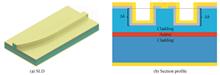
In order to optimize the performance of the 1 310 nm superluminescent diode, such as increase the output power of the device. In this simulation, the parameters of waveguide structure, and the heat dissipation for 1 310 nm superluminescent diode with the J-type waveguide have been investigated. The research results show that the waveguide etching depth, bending angle and thickness of the insulating layer were important for achieve high power output. Based on the research results, the superluminescent diode device structure and fabrication process were optimized, and J-type superluminescent diode with a ridge width of 5 μm, a bending angle of 8°, an etching depth of 1.7 μm and an insulating layer thickness of 300 nm was prepared. The superluminescent diode with 1.5 mm straight waveguide length has realized a high output power (42.2 mW) and wide bandwidth (10 nm) under 500 mA continuous-wave operation at room temperature. In order to optimize the performance of the 1 310 nm superluminescent diode, such as increase the output power of the device. In this simulation, the parameters of waveguide structure, and the heat dissipation for 1 310 nm superluminescent diode with the J-type waveguide have been investigated. The research results show that the waveguide etching depth, bending angle and thickness of the insulating layer were important for achieve high power output. Based on the research results, the superluminescent diode device structure and fabrication process were optimized, and J-type superluminescent diode with a ridge width of 5 μm, a bending angle of 8°, an etching depth of 1.7 μm and an insulating layer thickness of 300 nm was prepared. The superluminescent diode with 1.5 mm straight waveguide length has realized a high output power (42.2 mW) and wide bandwidth (10 nm) under 500 mA continuous-wave operation at room temperature.
Acta Photonica Sinica
- Publication Date: Jun. 25, 2021
- Vol. 50, Issue 6, 179 (2021)


A Planar Artificial Compound Eye Based on Metalens Array
Li ZHOU, Xiaohu ZHANG, Xiaogang LIN, Chao GAO, and Yongcai GUO
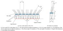
In order to realize an optical imaging system with light-weight, integration and large field of view, a planar artificial compound eye structure based on the utilization of a metalens array is proposed. It uses TiO2 nanopillars with different orientation angles to manipulate the electro-magnetic wave based on the grometric phase principles. It makes the surface of the metalens array and the image plane both planar, and does not need the non-spherical processing required by the traditional curved compound eyes. With the superposition of the off-axis phase onto the traditional matalens’ focusing phase, the effect produced by the illumination of the non-paraxial light beams on the imaging quality is effectively canceled and a large field of view is achieved. The designed compound eye is mainly composed of an array of 11×11 metalenses. It has the size of the 165 μm×165 μm and overall height of 18.6 μm, with the field of view of 140°×140°. The simulation results indicates that the the proposed compound eye structure achieves good image quality even under the illumination at a large off-axis angle (50°). In order to realize an optical imaging system with light-weight, integration and large field of view, a planar artificial compound eye structure based on the utilization of a metalens array is proposed. It uses TiO2 nanopillars with different orientation angles to manipulate the electro-magnetic wave based on the grometric phase principles. It makes the surface of the metalens array and the image plane both planar, and does not need the non-spherical processing required by the traditional curved compound eyes. With the superposition of the off-axis phase onto the traditional matalens’ focusing phase, the effect produced by the illumination of the non-paraxial light beams on the imaging quality is effectively canceled and a large field of view is achieved. The designed compound eye is mainly composed of an array of 11×11 metalenses. It has the size of the 165 μm×165 μm and overall height of 18.6 μm, with the field of view of 140°×140°. The simulation results indicates that the the proposed compound eye structure achieves good image quality even under the illumination at a large off-axis angle (50°).
Acta Photonica Sinica
- Publication Date: Jun. 25, 2021
- Vol. 50, Issue 6, 168 (2021)
Bifurcation-tunable Diffractionless Light Propagation in One-dimensional Non-Hermitian Photonic Lattice
Zhenjuan LIU, Haohao WANG, Yanan DAI, Zhiqing ZHANG, Yishan WANG, and Xinyuan QI
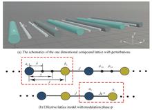
The light bifurcation transmission without diffraction in one-dimensional periodic compound photonic lattice was studied theoretically and numerically. When the lattice equals to degenerated Su-Schrieffer-Heeger model, the incident light with the wave number k=±π will bifurcate into two symmetric branches without any diffractionand the angles between two beams can be controlled by the coupling J between two lattice sites. In addition, a modulation phase ϕ is introduced. When the non-Hermitian perturbations satisfy the parity-time symmetry, the diffractionless light bifurcation phenomenon with any incident light wave can be realized as long as the incident wave vector k and the modulation phase ϕ respect the expression k+ϕ=±π. Further studies have shown that the next-nearest coupling can control the transmission angle and power division of two branches. This research provides new ideas for the design of optical switches and future all-optical paths. The light bifurcation transmission without diffraction in one-dimensional periodic compound photonic lattice was studied theoretically and numerically. When the lattice equals to degenerated Su-Schrieffer-Heeger model, the incident light with the wave number k=±π will bifurcate into two symmetric branches without any diffractionand the angles between two beams can be controlled by the coupling J between two lattice sites. In addition, a modulation phase ϕ is introduced. When the non-Hermitian perturbations satisfy the parity-time symmetry, the diffractionless light bifurcation phenomenon with any incident light wave can be realized as long as the incident wave vector k and the modulation phase ϕ respect the expression k+ϕ=±π. Further studies have shown that the next-nearest coupling can control the transmission angle and power division of two branches. This research provides new ideas for the design of optical switches and future all-optical paths.
Acta Photonica Sinica
- Publication Date: Apr. 25, 2021
- Vol. 50, Issue 4, 128 (2021)
Second-order Microcavity Length Based on Top-emitting Organic Light-emitting Diodes
Zhen WANG, Zhenshan LIANG, Fei XIAO, Jiawen CHEN, Yongsheng LU, Yue PENG, Wenxia ZHANG, and Yuchan WANG
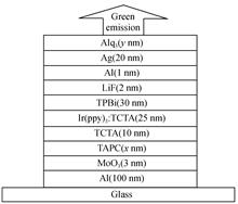
A Top-Emitting Organic Light-Emitting Diodes (TEOLEDs) with the configurations of Al (100 nm)/TAPC (x nm)/TCTA (10 nm)/TCTA:Ir(ppy)3 (10%, 25 nm)/TPBi (30 nm)/LiF (2 nm)/Al (1 nm)/Ag (20 nm)/Alq3 (y nm) (x=30, 130, 160, 170 and 180) (y=20, 40, 60 and 80) was fabricated. The experiments illustrate that photoelectric performance of the device can be improved by changing the thickness of the hole transport layer, which make the length of the device microcavity was in the enhancement zone of second-order microcavity effect. Moreover, by changing the light output coupling layer of the device, the transmittance and reflectance of the cathode of the device were changed, which can effectively improve the photoelectric performance of the device. A green TEOLEDs with the best photoelectric performance is achieved when the length of microcavity is 230 nm and the thickness of optical output coupling is 80 nm. The peak luminance, peak current efficiency and peak power efficiency of the TEOLEDs reach 25 960 cd/m2, 19.1 cd/A and 16.01 lm/W, respectively. A Top-Emitting Organic Light-Emitting Diodes (TEOLEDs) with the configurations of Al (100 nm)/TAPC (x nm)/TCTA (10 nm)/TCTA:Ir(ppy)3 (10%, 25 nm)/TPBi (30 nm)/LiF (2 nm)/Al (1 nm)/Ag (20 nm)/Alq3 (y nm) (x=30, 130, 160, 170 and 180) (y=20, 40, 60 and 80) was fabricated. The experiments illustrate that photoelectric performance of the device can be improved by changing the thickness of the hole transport layer, which make the length of the device microcavity was in the enhancement zone of second-order microcavity effect. Moreover, by changing the light output coupling layer of the device, the transmittance and reflectance of the cathode of the device were changed, which can effectively improve the photoelectric performance of the device. A green TEOLEDs with the best photoelectric performance is achieved when the length of microcavity is 230 nm and the thickness of optical output coupling is 80 nm. The peak luminance, peak current efficiency and peak power efficiency of the TEOLEDs reach 25 960 cd/m2, 19.1 cd/A and 16.01 lm/W, respectively.
Acta Photonica Sinica
- Publication Date: Apr. 25, 2021
- Vol. 50, Issue 4, 120 (2021)

Digital Thermo-optic Switch of SOI Waveguide Based on Goos-Hänchen Spatial Shift of Reflected Mode
Zhuo CHEN, Tiancheng LI, Degui SUN, Na SUN, Hongpeng SHANG, and Chen CHEN
With the waveguide corner mirror structure and the effective combination of the Goos-Hanchen (GH) spatial shift and the thermo-optical effect refractive index modulation, a digital thermo-optical switch structure of waveguide reflected mode is proposed. The GH spatial shift is optimized under the condition of a given incident angle, and the reflected beam has a larger jump under an eigenstate with the GH effect. On a silicon-on-insulator platform with a 1.0 μm thick silicon film, the guided mode eigenstate matching between the single-mode input waveguide and the multimode interference waveguide structure verifies the function of a 1×3 digital optical switch. In experiment, the optical loss caused by the device structure is 0.3 dB, the switching power is 130~150 mW, the switching time is about 50 μs, and the isolation between adjacent output ports is 15 dB. The comparison with the latest results of the Mach-Zehnder interferometer 2×2 thermo-optic switch and the newly emerging plasma effect thermo-optic switch shows the advancement of this digital TO switch. With the waveguide corner mirror structure and the effective combination of the Goos-Hanchen (GH) spatial shift and the thermo-optical effect refractive index modulation, a digital thermo-optical switch structure of waveguide reflected mode is proposed. The GH spatial shift is optimized under the condition of a given incident angle, and the reflected beam has a larger jump under an eigenstate with the GH effect. On a silicon-on-insulator platform with a 1.0 μm thick silicon film, the guided mode eigenstate matching between the single-mode input waveguide and the multimode interference waveguide structure verifies the function of a 1×3 digital optical switch. In experiment, the optical loss caused by the device structure is 0.3 dB, the switching power is 130~150 mW, the switching time is about 50 μs, and the isolation between adjacent output ports is 15 dB. The comparison with the latest results of the Mach-Zehnder interferometer 2×2 thermo-optic switch and the newly emerging plasma effect thermo-optic switch shows the advancement of this digital TO switch.
Acta Photonica Sinica
- Publication Date: Apr. 25, 2021
- Vol. 50, Issue 4, 111 (2021)

White Lght Emission from the Tb3+/Eu3+ Co-doped All-inorganic Halide Perovskite Quantum Dots in Ambient Air
Rui ZHANG, Jianfeng ZHANG, Yaoxin YUAN, Haiyun LIU, Gang CHEN, Mengqing HONG, Fengfeng LUO, and Wen YANG
In order to overcome the shortcomings in obtaining white light emission due to the anion exchange reaction from different halide perovskite quantum dots and unstable red light emission halide perovskite quantum dots, a method was used to prepare rare earth ions Tb3+/Eu3+ co-doping into perovskite quantum dots in ambient air. By adjusting the doping ratio of Tb3+/Eu3+ rare earth ions, the energy transfer from the host lattice of perovskite quantum dots to Tb3+/Eu3+ was accordingly manipulated to obtain single-component and white light emission perovskite quantum dots of (Tb, Eu)∶CsPbCl3 and (Tb,Eu)∶CsPb(Cl/Br)3. Meanwhile, we delicately investigated the morphology, structure, luminescence performance, energy transfer mechanism and stability of quantum dots. The results show that under 365 nm laser excitation, white light emission with 1 931 Commission Internationale de l’Eclairage color coordinates was achieved in perovskite quantum dots (Tb, Eu):CsPbCl3 with different contents of Tb3+/Eu3+ ions. When the feed ratio PbCl2∶TbCl3∶EuCl3 is 1∶1.5∶1, the quantum yield is 3.59%, which is 6 times higher than the quantum yield (0.57%) of pure CsPbCl3 quantum dots. Further research found that the (Tb, Eu)∶CsPbCl3 quantum dots were stored in the air for 2 months, the quantum yield was almost unchanged (3.63%), maintaining good stability. Moreover, the luminescence characteristics of the co-doped perovskite quantum dots with Tb3+ and Eu3+ synthesized with different solvents (n-octane, 1-octadecene) were compared. Tb3+/Eu3+ co-doped perovskite quantum dots (Tb, Eu): CsPbCl3 ware used to achieve single-component white light emission with good stability and has certain application prospects. In order to overcome the shortcomings in obtaining white light emission due to the anion exchange reaction from different halide perovskite quantum dots and unstable red light emission halide perovskite quantum dots, a method was used to prepare rare earth ions Tb3+/Eu3+ co-doping into perovskite quantum dots in ambient air. By adjusting the doping ratio of Tb3+/Eu3+ rare earth ions, the energy transfer from the host lattice of perovskite quantum dots to Tb3+/Eu3+ was accordingly manipulated to obtain single-component and white light emission perovskite quantum dots of (Tb, Eu)∶CsPbCl3 and (Tb,Eu)∶CsPb(Cl/Br)3. Meanwhile, we delicately investigated the morphology, structure, luminescence performance, energy transfer mechanism and stability of quantum dots. The results show that under 365 nm laser excitation, white light emission with 1 931 Commission Internationale de l’Eclairage color coordinates was achieved in perovskite quantum dots (Tb, Eu):CsPbCl3 with different contents of Tb3+/Eu3+ ions. When the feed ratio PbCl2∶TbCl3∶EuCl3 is 1∶1.5∶1, the quantum yield is 3.59%, which is 6 times higher than the quantum yield (0.57%) of pure CsPbCl3 quantum dots. Further research found that the (Tb, Eu)∶CsPbCl3 quantum dots were stored in the air for 2 months, the quantum yield was almost unchanged (3.63%), maintaining good stability. Moreover, the luminescence characteristics of the co-doped perovskite quantum dots with Tb3+ and Eu3+ synthesized with different solvents (n-octane, 1-octadecene) were compared. Tb3+/Eu3+ co-doped perovskite quantum dots (Tb, Eu): CsPbCl3 ware used to achieve single-component white light emission with good stability and has certain application prospects.
Acta Photonica Sinica
- Publication Date: Mar. 25, 2021
- Vol. 50, Issue 3, 86 (2021)
Preparation and Properties of Flexible Liquid Crystal Micro-lens Arrays
Penghui LIU, Shiyao LI, Wenwen WANG, Xuyang WENG, Chaoxing WU, Xiongtu ZHOU, and Yongai ZHANG
A Flexible Liquid Crystal Micro-Lens Arrays (LC MLAs) with an adjustable focal length was designed and prepared to solve the narrow viewing angle of the integrated imaging. In this paper, the hole-patterned driven- electrode arrays were fabricated by a photolithography technology and the flexible Polyimide (PI) film was prepared by a spin coating method on the flexible ITO glass substrate. After the PI film layer was heated at 60°C for 5 min, the PI orientation layer was formed by using the plasma at a power of 630 W for 5 minutes. The optical properties of LC MLAs with a flat substrate and a curvature radius of 7.5cm were studied after the LC MLAs were fabricated. The experimental results show that the prepared LC MLAs can achieve the excellent focusing properties under the condition of a flat plate and a curvature radius of 7.5 cm. The interference patterns are uniform and the focal radius are small when the operating voltages are applied to the LC MLAs. Further, the focal length of the flexible LC MLAs with the curvature radius of 7.5 cm can be tunable from 0.43 mm to 1.05 mm when the operating voltages are changed from 3 Vrms to 5.3 Vrms. A Flexible Liquid Crystal Micro-Lens Arrays (LC MLAs) with an adjustable focal length was designed and prepared to solve the narrow viewing angle of the integrated imaging. In this paper, the hole-patterned driven- electrode arrays were fabricated by a photolithography technology and the flexible Polyimide (PI) film was prepared by a spin coating method on the flexible ITO glass substrate. After the PI film layer was heated at 60°C for 5 min, the PI orientation layer was formed by using the plasma at a power of 630 W for 5 minutes. The optical properties of LC MLAs with a flat substrate and a curvature radius of 7.5cm were studied after the LC MLAs were fabricated. The experimental results show that the prepared LC MLAs can achieve the excellent focusing properties under the condition of a flat plate and a curvature radius of 7.5 cm. The interference patterns are uniform and the focal radius are small when the operating voltages are applied to the LC MLAs. Further, the focal length of the flexible LC MLAs with the curvature radius of 7.5 cm can be tunable from 0.43 mm to 1.05 mm when the operating voltages are changed from 3 Vrms to 5.3 Vrms.
Acta Photonica Sinica
- Publication Date: Mar. 25, 2021
- Vol. 50, Issue 3, 78 (2021)
Same Side Arrayed Waveguide Grating Multiplexer for Data Center Transmitter
Liangliang WANG, Jiashun ZHANG, Junming AN, Yanzhang HU, and Chongxin SHAN
A silicon based optical waveguide with 1.5% refractive index difference is used for data center interconnect on wavelength-division multiplexing chip. A 4-channel chip with same side, small size and low loss is designed and fabricated for data center transmitter. The size of the chip is 6.6 mm×2.2 mm, the minimum insertion loss is less than 2.33 dB, the 1 dB bandwidth is more than 11.35 nm, the polarization dependent loss is less than 0.14 dB, and the wavelength accuracy deviation is less than 0.38 nm. The optical performance can meet the wavelength-division multiplexing commercial specifications of the data center optical interconnect. A silicon based optical waveguide with 1.5% refractive index difference is used for data center interconnect on wavelength-division multiplexing chip. A 4-channel chip with same side, small size and low loss is designed and fabricated for data center transmitter. The size of the chip is 6.6 mm×2.2 mm, the minimum insertion loss is less than 2.33 dB, the 1 dB bandwidth is more than 11.35 nm, the polarization dependent loss is less than 0.14 dB, and the wavelength accuracy deviation is less than 0.38 nm. The optical performance can meet the wavelength-division multiplexing commercial specifications of the data center optical interconnect.
Acta Photonica Sinica
- Publication Date: Jan. 25, 2021
- Vol. 50, Issue 1, 165 (2021)
Investigation on the Preparation of High Precision Multilayer X-ray Fresnel Zone Plates Based on Atomic Layer Deposition Technology
Lujie WU, Qingtao WEN, Yazeng GAO, Weier LU, Yang XIA, Yanli LI, Xiangdong KONG, and Li HAN
Based on the process of combining atomic layer deposition and focused ion beam cutting and polishing, a multi-layer film-type wave zone plate preparation technology was proposed. Firstly, using the coupled wave theory, it is calculated that the outermost ring width of Al2O3/HfO2, Al2O3/SiO2, Al2O3/Ir and Al2O3/Ta2O5 four material combinations of multi-layer film band plates with X-ray energy of 8 keV and the theoretical diffraction efficiency of the Fresnel zone plate at 15 keV. The influence of the width of the outermost ring and the height of the zone plate on the diffraction efficiency was discussed, and Al2O3/HfO2 was selected as the subsequent laminate preparation. The growth characteristics of Al2O3 and HfO2 films prepared by atomic layer deposition were studied, and the feasibility of preparing single-layer film thickness of 10 nm by atomic layer deposition technology was verified. The experimental results showed that the preparation of Al2O3 and HfO2 films by atomic layer deposition technology was rough The degree of control is 1 nm, the uniformity is better than 1.5%, and the thickness error of the single stack is only 0.416 nm. At the same time, a high-resolution X-ray Fresnel zone plate with an outermost ring width of 10 nm and an aspect ratio of 200 was obtained using focused ion beam cutting and polishing technology. Based on the process of combining atomic layer deposition and focused ion beam cutting and polishing, a multi-layer film-type wave zone plate preparation technology was proposed. Firstly, using the coupled wave theory, it is calculated that the outermost ring width of Al2O3/HfO2, Al2O3/SiO2, Al2O3/Ir and Al2O3/Ta2O5 four material combinations of multi-layer film band plates with X-ray energy of 8 keV and the theoretical diffraction efficiency of the Fresnel zone plate at 15 keV. The influence of the width of the outermost ring and the height of the zone plate on the diffraction efficiency was discussed, and Al2O3/HfO2 was selected as the subsequent laminate preparation. The growth characteristics of Al2O3 and HfO2 films prepared by atomic layer deposition were studied, and the feasibility of preparing single-layer film thickness of 10 nm by atomic layer deposition technology was verified. The experimental results showed that the preparation of Al2O3 and HfO2 films by atomic layer deposition technology was rough The degree of control is 1 nm, the uniformity is better than 1.5%, and the thickness error of the single stack is only 0.416 nm. At the same time, a high-resolution X-ray Fresnel zone plate with an outermost ring width of 10 nm and an aspect ratio of 200 was obtained using focused ion beam cutting and polishing technology.
Acta Photonica Sinica
- Publication Date: Jan. 25, 2021
- Vol. 50, Issue 1, 156 (2021)
Design of Metasurface Lens with Two Focal Spots Based on Polarization Response
Peng-jiu ZHAO, Shou-peng LIU, Yu LUO, Wei REN, and Xiao-hu CHEN
A focusing lense with two focal spots based on dielectric metasurface was designed which can extend the focus axially. The device modulates the propagation phase and the geometric phase at the same time and realizes the independent control of a group of orthogonal polarized incident light by varying the aspect ratio and the rotation angle of the titanium dioxide pillars. The designed metasurface focuses the left-handed and right-handed circularly polarized light at contiguous positions to extend the focus axially. We extend the length of focus twice as initial value at 650 nm wavelength and maintain the lateral width of the focus in the meantime. The optimization of the focus shape and the switch of focus position with different focal lengths can be realized by adjusting the incident light into an elliptically polarized light. A focusing lense with two focal spots based on dielectric metasurface was designed which can extend the focus axially. The device modulates the propagation phase and the geometric phase at the same time and realizes the independent control of a group of orthogonal polarized incident light by varying the aspect ratio and the rotation angle of the titanium dioxide pillars. The designed metasurface focuses the left-handed and right-handed circularly polarized light at contiguous positions to extend the focus axially. We extend the length of focus twice as initial value at 650 nm wavelength and maintain the lateral width of the focus in the meantime. The optimization of the focus shape and the switch of focus position with different focal lengths can be realized by adjusting the incident light into an elliptically polarized light.
Acta Photonica Sinica
- Publication Date: Jan. 01, 2020
- Vol. 49, Issue 9, 0923002 (2020)
Topics
© Copyright 2018-2021 | Chinese Laser Press. All Rights Reserved 沪ICP备15018463号-20